Imager basics
For the foreseeable future, there will be a significant role for both types of sensor in imaging. The most successful users of advanced image capture technology will be those who consider not only the base technology, but also the sustainability, adaptability and support. They will perform the best long term in a dynamic technology environment that the battle between CCDs and CMOS promises to deliver.
Both image sensors are pixelated metal oxide semiconductors. They accumulate signal charge in each pixel proportional to the local illumination intensity, serving a spatial sampling function.
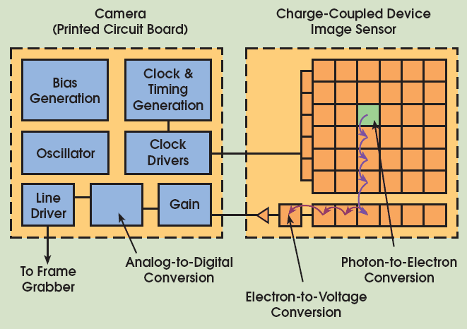
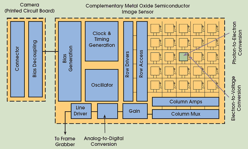
When exposure is complete, a CCD (Figure 1) transfers each pixel's charge packet sequentially to a common output structure, which converts the charge to a voltage, buffers it and sends it off-chip. In a CMOS imager (Figure 2), the charge-to-voltage conversion takes place in each pixel. This difference in readout techniques has significant implications for sensor architecture, capabilities and limitations.
|
Figure 1. On a CCD, most functions take place on the camera's printed circuit board. If the application's demands change, a designer can change the electronics without redesigning the imager. |  |
Eight attributes characterize imagesensor performance:
However, feedback-based amplifier structures can trade off gain for greater uniformity under illumination. The amplifiers have made the illuminated uniformity of some CMOS imagers closer to that of CCDs, sustainable as geometries shrink.
Still lacking, though, is offset variation of CMOS amplifiers, which manifests itself as nonuniformity in darkness. While CMOS imager manufacturers have invested considerable effort in suppressing dark nonuniformity, it is still generally worse than that of CCDs. This is a significant issue in high-speed applications, where limited signal levels mean that dark nonuniformities contribute significantly to overall image degradation.
Implementing uniform electronic shuttering in CMOS imagers requires a number of transistors in each pixel. In line-scan CMOS imagers, electronic shuttering does not compromise fill factor because shutter transistors can be placed adjacent to the active area of each pixel. In areascan (matrix) imagers, uniform electronic shuttering comes at the expense of fill factor because the opaque shutter transistors must be placed in what would otherwise be an optically sensitive area of each pixel. CMOS matrix sensor designers have dealt with this challenge in two ways:
A nonuniform shutter, called a rolling shutter, exposes different lines of an array at different times. It reduces the number of in-pixel transistors, improving fill factor. This is sometimes acceptable for consumer imaging, but in higher-performance applications, object motion manifests as a distorted image.
| Choose Your Imager CMOS imagers offer superior integration, power dissipation and system size at the expense of image quality (particularly in low light) and flexibility. They are the technology of choice for high-volume, spaceconstrained applications where image quality requirements are low. This makes them a natural fit for security cameras, PC videoconferencing, wireless handheld device videoconferencing, bar-code scanners, fax machines, consumer scanners, toys, biometrics and some automotive invehicle uses. CCDs offer superior image quality and flexibility at the expense of system size. They remain the most suitable technology for high-end imaging applications, such as digital photography, broadcast television, high-performance industrial imaging, and most scientific and medical applications. Furthermore, flexibility means users can achieve greater system differentiation with CCDs than with CMOS imagers. Sustainable cost between the two technologies is approximately equal. This is a major contradiction to the traditional marketing pitch of virtually all of the solely CMOS imager companies. |
A uniform synchronous shutter, sometimes called a nonrolling shutter, exposes all pixels of the array at the same time. Object motion stops with no distortion, but this approach consumes pixel area because it requires extra transistors in each pixel. Users must choose between low fill factor and small pixels on a small, less-expensive image sensor, or large pixels with much higher fill factor on a larger, more costly image sensor.
| Figure 2. A CMOS imager converts charge to voltage at the pixel, and most functions are integrated into the chip. This makes imager functions less flexible but, for applications in rugged environments, a CMOS camera can be more reliable. |
 |
Reliability
Both image chip types are equally reliable in most consumer and industrial applications. In ultrarugged environments, CMOS imagers have an advantage because all circuit functions can be placed on a single integrated circuit chip, minimizing leads and solder joints, which are leading causes of circuit failures in extremely harsh environments.
CMOS image sensors also can be much more highly integrated than CCD devices. Timing generation, signal processing, analog-to-digital conversion, interface and other functions can all be put on the imager chip. This means that a CMOS-based camera can be significantly smaller than a comparable CCD camera.
The user needs to consider, however, the cost of this integration. CMOS imagers are manufactured in a wafer fabrication process that must be tailored for imaging performance. These process adaptations, compared with a nonimaging mixed-signal process, come with some penalties in device scaling and power dissipation. Although the pixel portion of the CMOS imager almost invariably has lower power dissipation than a CCD, the power dissipation of other circuits on the device can be higher than that of a CCD using companion chips from optimized analog, digital and mixed signal processes. At a system level, this calls into question the notion that CMOS-based cameras have lower power dissipation than CCDbased cameras. Often, CMOS is better, but it is not unequivocally the case, especially at high speeds (above about 25-MHz readout).
The other significant considerations in system integration are adaptability, flexibility and speed of change. Most CMOS image sensors are designed for a large, consumer or near-consumer application. They are highly integrated and tailored for one or a few applications. A system designer should be careful not to invest fruitlessly in attempting to adapt a highly application-specific device for a use to which it is not suited.
CCD image sensors, on the other hand, are more general purpose. The pixel size and resolution are fixed in the device, but the user can easily tailor other aspects such as readout speed, dynamic range, binning, digitizing depth, nonlinear analog processing and other customized modes of operation.
Even when it makes economic sense to pay for sensor customization to suit an application, time to market can be an issue. Because CMOS imagers are systems on a chip, development time averages 18 months, depending on how many circuit functions the designer can reuse from previous designs in the same wafer fabrication process. And this amount of time is growing because circuit complexity is outpacing design productivity. This compares with about eight months for new CCD designs in established manufacturing processes. CCD systems can also be adapted with printed circuit board modifications, whereas fully integrated CMOS imaging systems require new wafer runs.
Which costs less?
One of the biggest misunderstandings about image sensors is cost.
Many early CMOS proponents argued that their technology would be vastly cheaper because it could be manufactured on the same high-volume wafer processing lines as mainstream logic and memory devices. Had this assumption proved out, CMOS would be cheaper than CCDs.
However, the accommodations required for good electro-optical performance mean that CMOS imagers must be made on specialty, lowervolume, optically adapted mixed-signal processes and production lines.
This means that CMOS and CCD image sensors do not have significantly different costs when produced in similar volumes and with comparable cosmetic grading and silicon area. Both technologies offer appreciable volumes, but neither has such commanding dominance over the other to establish untouchable economies of scale.
CMOS may be less expensive at the system level than CCD, when considering the cost of related circuit functions such as timing generation, biasing, analog signal processing, digitization, interface and feedback circuitry. But it is not cheaper at a component level for the pure image sensor function itself.
The larger issue around pricing, particularly for CMOS users, is sustainability. Many CMOS startups are dedicated to high-volume applications. Pursuing the highest-volume applications from a small base of business has meant that these companies have had to price below their costs to win business in commodity markets. Some start-ups will win and sustain these prices. Others will not and will have to raise prices. Still others will fail entirely.
CMOS users must be aware of their suppliers' profitability and cost structure to ensure that the technology will be sustainable. The customer's interest and the venture capitalist's interest are not well-aligned: Investors want highest return, even if that means highest risk, whereas customers need stability because of the high cost of midstream system design change.
Increasingly, money and talent are flowing to CMOS imaging,in large part because of the high-volume applications enabled by the small imaging devices and the high digital processing speeds. Over time, CMOS imagers should be able to advance into higher-performance applications.
For the moment, CCDs and CMOS remain complementary technologies - one can do things uniquely that the other cannot. Over time, this stark distinction will soften, with CMOS imagers consuming more and more of the CCD's traditional applications. But this process will take the better part of a decade - at the very least.
Meet the author
Dave Litwiller is Vice President, Corporate Marketing at DALSA in Waterloo, Ontario, Canada.